
S9014 BjT - 45V 100mA NPN Bipolar Transistors
| Manufacturer: | HXY MOSFET |
| SKU: | S18405 |
| Manufacturer | HXY MOSFET |
| brand | HXY MOSFET |
| collector-emittervceo | 45V |
| easyeda-id | C920324 |
| mounting | SMD/SMT |
| package-size | SOT-23 |
| power-dissipation | 200mW |
VBZM150N03 N-Channel 30V (D-S) MOSFET
এটি একটি শক্তিশালী N-Channel 30V MOSFET, যা বিশেষভাবে DC/DC কনভার্টার, UPS/IPS এবং OR-ing এর মতো অ্যাপ্লিকেশনে ব্যবহারের জন্য ডিজাইন করা হয়েছে। এর DT-Trench Power MOSFET প্রযুক্তি হাই পারফরম্যান্স এবং ইফিসিয়েন্সি নিশ্চিত করে। প্রোডাক্টটি RoHS Directive 2011/65/EU অনুসারে কমপ্লায়েন্ট এবং প্রতিটি ইউনিট Rg ও UIS টেস্টেড।
Simplified Schematic

VBZM150N03 একটি হাই কুয়ালিটি N-Channel MOSFET যা 30VDS ড্রেন সোর্স ভোল্টেজ এবং 140A পর্যন্ত ড্রেন কারেন্ট সাপোর্ট করে। এর গেট-সোর্স ভোল্টেজ (VGS) ±20V পর্যন্ত সহ্য করতে পারে, যা কন্ট্রোলিং এবং ড্রাইভিং সার্কিটের স্থায়িত্ব নিশ্চিত করে এবং ইন্সট্যান্টেনিয়াস লোডের ক্ষেত্রে খুবই উপযোগী।
Absolute Maximum Ratings
Parameter | Symbol | Rating (Max) | Units | |
|---|---|---|---|---|
Drain-Source Voltage | VDS | 30 | V | |
Gate-Source Voltage | VGS | ±10 | ||
Continuous Drain Current, (TJ =175℃) | TC=25℃ | ID | 140 a, e | A |
TC=70℃ | 110e | |||
TA=25℃ | 39b, c | |||
TA=70℃ | 28b, c | |||
Continuous Source-Drain Diode Current | TC=25℃ | IS | ||
TA=25℃ | ||||
Pulsed Drain Current | IDM | 370 | ||
Avalanche Current Pulse | L = 0.1 mH | IAS | 39 | |
Single Pulse Avalanche Energy | EAS | 375 | mJ | |
Maximum Power Dissipation | TC=25℃ | PD | 250a | W |
TC=70℃ | 175 | |||
TA=25℃ | ||||
TA=70℃ | ||||
Storage and Junction Temperature Range | TSTG, TJ | -55 to 175 | ℃ |
এগুলো শুধুমাত্র স্ট্রেস রেটিং। এর বেশি হলে মস্ফেটটি পুড়ে যেতে পারে।
Specifications of VBZM150N03 MOSFET
Parameter | Symbol | Test Conditions | Min | Typ. | Max | Unit |
|---|---|---|---|---|---|---|
Drain-Source Breakdown Voltage | VDS | VGS = 0 V, ID = 250 µA | 30 | ---- | ---- | V |
Temperature Coefficient | ∆VDS/TJ | ID = 250 µA | ---- | 35 | ---- | mV/°C |
Temperature Coefficient | ∆VGS/TJ | ---- | -7.5 | ---- | ||
Gate-Source Threshold Voltage | VGS(th) | VDS = VGS, ID = 250 µA | 1.0 | ---- | 3.0 | V |
Gate-Source Leakage | IGSS | VDS = 0 V, VGS = ± 20 V | ---- | ---- | ±100 | nA |
Zero Gate Voltage Drain Current | IDSS | VDS = 0 V, VGS = ± 20 V | ---- | ---- | 1 | µA |
VDS = 24 VGS = 0 V, TJ = 55 °C | ---- | ---- | 10 | |||
On-State Drain Currentf | ID(on) | VDS ≥5 V, VGS = 10 V | 90 | ---- | ---- | A |
Forward Transconductanceg | gFS | VDS = 15 V, ID = 38.8 A | ---- | 160 | ---- | S |
Drain-Source On-State Resistancef | RDS(on) | VGS = 10 V, ID = 38.8 A | ---- | 0.0020 | ---- | Ω |
VGS = 4.5 V, ID = 37 A | 0.0028 |
Parameter
Symbol
Test Conditions
Min
Typ
Max
Unit
Input Capacitance
CISS
VDS = 15 V, VGS = 0 V, f = 1 MHz
----
8400
----
pF
Output Capacitance
COSS
----
1725
----
Reverse Transfer Capacitance
CRSS
----
970
----
Total Gate Charge
QG
VDS = 15 V, VGS = 10 V, ID = 38.8 A----
171
257
nC
VDS = 15 V, VGS = 4.5 V, ID = 28.8 A
----
81.5
123
Gate-Source Charge
QGS
----
34
----
Gate-Drain Charge
QGD
----
29
----
Gate Resistance
RG
f = 1 MHz
----
1.4
2.1
Ω
Turn-On Delay Time
tD(on)
VDD = 15 V, RL = 0.625 Ω ID ≅ 24 A, VGEN = 10 V, Rg = 1 Ω
----
18
27
nS
Rise Time
tR
11
17
Turn-Off Delay Time
tD(off)
70
105
Fall Time
tF
10
15
Turn-On Delay Time
tD(on)
VDD = 15 V, RL = 0.67 Ω ID ≅ 22.5 A, VGEN = 4.5 V, Rg = 1 Ω
----
55
83
Rise Time
tR
180
270
Turn-Off Delay Time
tD(off)
55
83
Fall Time
tF
12
18
Parameter
Symbol
Test Conditions
Min
Typ
Max
Unit
Input Capacitance
CISS
TC = 25°C
----
140
----
A
Pulse Diode Forward Currentf
ISM
----
----
370
----
Body Diode Voltage
VSD
IS = 22A
----
0.8
----
V
Body Diode Reverse Recovery Time
tRR
IF = 20 A, di/dt = 100 A/µs, TJ = 25 °C
----
52
78
nS
Body Diode Reverse Recovery Charge
QRR
----
70.2
105
nC
Reverse Recovery Fall Time
tRRF
----
27
----
nS
Reverse Recovery Rise Time
tRRR
----
25
----
Thermal Resistance Ratings
Note:
- Based on TC = 25 °C.
- Surface mounted on 1" x 1" FR4 board.
- t = 10 sec.
- Maximum under steady state conditions is 90 °C/W.
- Calculated based on maximum junction temperature. Package limitation current is 90 A.
- Pulse test; pulse width ≤ 300 µs, duty cycle ≤ 2%.
- Guaranteed by design, not subject to production testing.
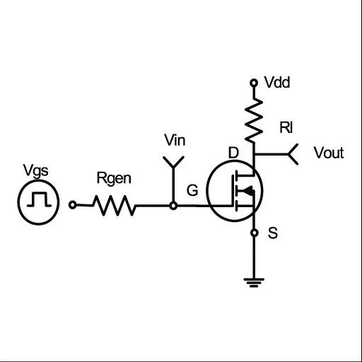
Figure 1: Switching test circuit
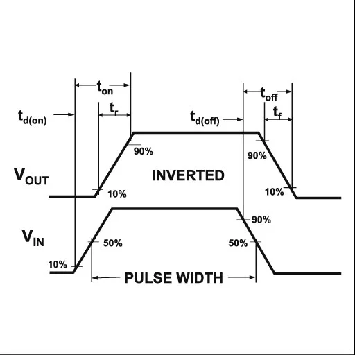
Figure 2: Switching Waveforms of AP4580